Reverse Engineering a GPU from 2009
With the recent efforts going into Asahi Linux, especially the GPU reverse engineering portion of it, I had the idea of trying to see if I could try something in that spirit on some hardware I own. After a bit of searching through old boxes I found a few old phones and some old desktop GPUs, the desktop ones mostly already work with the r600 and Nouveau drivers in mesa/linux, same goes for most of the mobiles devices, which have an assortment of Adreno and Mali GPUs, with a single exception.
My Galaxy Tab 2.0 7.0 (P3110) is based on the Texas Instruments OMAP 4430 SoC, which includes a PowerVR SGX540 by Imagination Technologies, this specific gpu belongs to their "Series5" generation. Anyone who's a bit familiar with the open source driver world probably knows that Imagination is well-known for only releasing binary drivers for their GPUs (even if they have recently started merging a Vulkan driver into mesa). Surprisingly enough the kernel side of the GPU driver is open source, so that will be quite helpful.
Another important part of this is that there was a large source code leak of driver code from the same era this GPU was released in, but due to the questionable legality of publishing information derived from it I decided to take a 100% clean reverse engineering approach.
Getting started
Let's see what the gpu is capable of, after a quick search we can see it supports OpenGL ES 2.0, this means that it has support for shaders. For those unfamiliar the rough overview of how 3D rendering usually works on computers is that the GPU gets sent a list of "primitives", primitives are generally triangles, squares, or strips of either, and turns them into pixels. This procedure used to be rather rigid back in the days of OpenGL 1.0, but as the need for more complex and realistic scenes arised "shaders" were introduced, shaders are essentially points in the primitive -> pixel transformation pipeline where a programmer can specify custom code to alter the results of rendering.
To be more specific, while rendering using OpenGL 2.0 the programmer has access to two kinds of shaders, Vertex shaders and Fragment shaders, vertex shaders are programs that run once for each vertex of each input primitive and output another (possibly modified) vertex, fragment shaders are programs that run once for each pixel covered by a primitive (think for instance the inside of a filled-in triangle). Vertex shaders are generally used to move or rotate objects around or perform deformations on them, while fragment shaders are usually used for lighting and texturing.
This means that just like most other programmable hardware GPUs have their own assembly language, and the most exciting part is that GPU assembly is in general a lot more unique than CPU assembly code, in general there are more degrees of freedom for design, for instance Intel GPUs have high level control-flow instructions (loops, if statements).
So this sets our first (and probably most important) goal, finding out exactly what the assembly code that runs on this GPU looks like.
First let's see if the manufacturer says anything useful about it, if we search for manufacturer-specific documentation we can find this pdf, which contains a very general block diagram of the GPU and some information about how 3D rendering works within it, of course not enough to accomplish anything useful at the moment. But there's some good initial information, first of all we now know the shader architecture is unified, that meaning that the vertex and fragment shaders both use the same assembly code (this is not true of a lot of older GPUs), secondly we can see that the GPU runs a "Microkernel", which apparently does interrupt handling.
They also seem to provide a "shader profiling tool", which can show the disassembly for shaders on PowerVR GPUs, but in their own words:

Well that wasn't much information, but definitely more than I expected them to reveal.
Getting to work
One thing that's quite important to this process is that the tablet is at the moment running Android (it is rooted and running a custom ROM), so all of the reverse engineering for now has to be done with Android in the way, and part of the test program has to be written in Java, in general Android ended up being the cause of a lot issues. One good thing is that google provides a very simple OpenGL ES example using the android Native Development Kit and C++ here.
The first step to reverse engineering an architecture is having binaries for it in the first place, which isn't as easy as it sounds. In OpenGL the main way to compile shaders is doing so at runtime and then linking them together into a "program". I did get a bit lucky since OpenGL ES 2.0 has an "OES_get_program_binary" extension which is supported by the driver implementation on Android (most likely meant to be used by 3D applications to cache shaders since mobile devices are quite limited in power), so getting program binaries is as easy as compiling them and calling "glGetProgramBinaryOES" with the program and other relevant data as an argument, the code for doing this is:
    GLint length = 0;
    glGetProgramiv(program, GL_PROGRAM_BINARY_LENGTH_OES, &length);
    std::vector<GLubyte> buffer(length);
    GLenum format = 0;
    glGetProgramBinaryOES(program, length, NULL, &format, buffer.data());
The shader code I used for the initial dump is the following:
auto gVertexShader =
    "attribute vec4 vPosition;\n"

    "void main() {\n"
      "  gl_Position = vPosition;"
    "}\n";

auto gFragmentShader =
    "precision mediump float;\n"

    "void main() {\n"
        "  gl_FragColor = vec4(1.0, 1.0, 0.0, 1.0);\n"
    "}\n";
These are trivial shaders, one simply passes the position through for every vertex, the other sets a fixed color for every pixel.
Now we can write our buffer to disk and open it up in a hex editor:
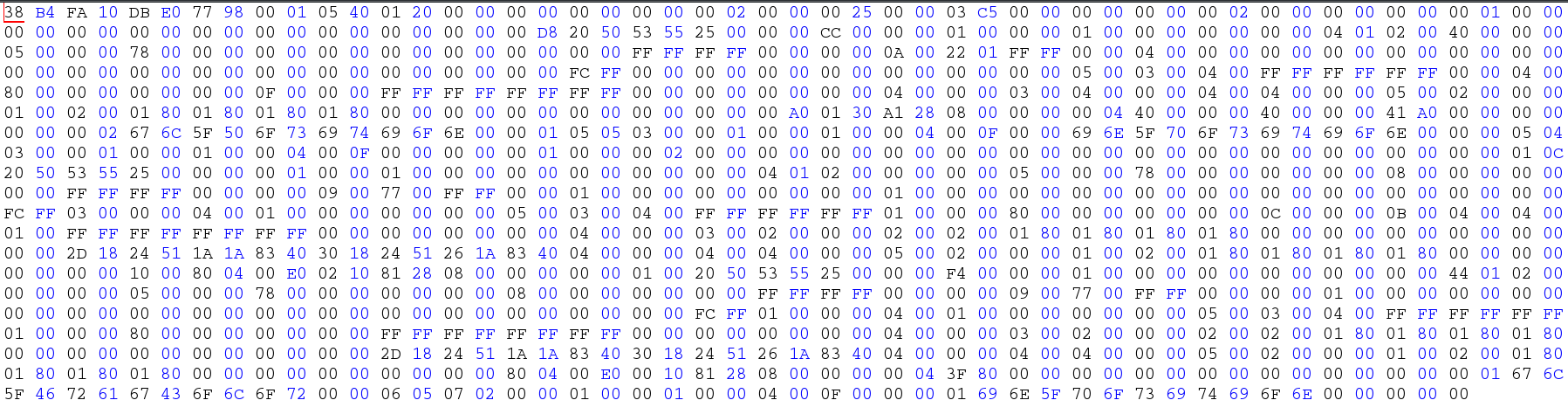
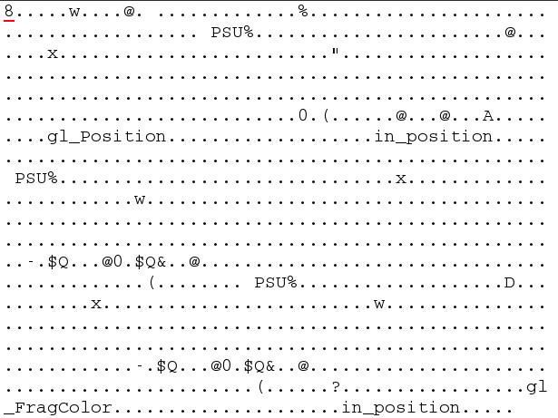
The first thing we can see here is that there's some strings that refer to variables present in the vertex shaders, specifically to inputs and output variables, additionally we can see some repeating "PSU%" bytes, which may be part of some sort of header for shaders (this is a program binary, so it contains both a vertex and a fragment shader)
At this point to figure out more about this we should start doing some differential testing, that is loading two slightly different shaders and comparing the output binaries.
This is also where we meet our first driver bug, the binary returned by glGetProgramBinaryOES is "fixed" per-app installation and changing it requires uninstalling the app and reinstalling it every time I need to test it, why and how it got through this happens is beyond me, it didn't end up being as annoying as it might sound but it did slow down my progress.
Let's make a rather trivial change to the vertex shader:
auto gVertexShader =
    "attribute vec4 vPosition;\n"

    "void main() {\n"
      "  gl_Position = vPosition + (0.34, 0.72, 0.55, 0.982);"
    "}\n";
These values were picked for a few reasons, GPUs tend to have instructions that work on registers that hold more than one value in them (SIMD), there's some chance that if I had picked the same value for every component (for instance (1.0, 1.0, 1.0, 1.0)) of the vector the resulting assembly might look something like this:
load r0, (address)
splat v0, r0
add (result register), v0, v1
Where v1 here is assumed to hold the input vertex data, and the "splat" operation writes the value of a single-element register to each of the elements of a multi-element (vector) one, by picking different values if the GPU works anything like this it will probably generate a load instruction that reads an entire vector and an add instead.
From the hexadeimal diff we can tell a few things, first of all even if one of the two shaders changed the initial portion stayed the same minus a few changes.
The 4 bytes after the initial 4 bytes (which are almost surely a signature) look like they could be a hash, the following 20 bytes are also unaltered. The next change is at this offset, but if we inspect it more closely we can see that the actual numerical value did not really vary a lot. In fact if we check the length of the rest of the file starting at the byte after this value we see that it is exactly the numerical value in these 4 bytes. I am not sure exactly why they encode it here and not elsewhere (for instance encoding the lengths of singular shaders / "variable blocks"), but with this information on hand we can look for more instances of this later.
Another important thing to check is which section of the data stayed the same after this alteration, this is a bit annoying to check by eye because the data is sequential in encoding but it semantically has many smaller variable-length sections. But due to seemingly having a somewhat fixed header we can notice another thing, there's another length field that ends exactly before data that is exactly our floating point constants in hexadecimal. We could attempt to find the same exact kind of structure for fragment shaders, but since it is most likely similar I chose to write a small extractor for the vertex shader code.
After taking a look at some vertex shaders in this format and decompiling the code for glShaderBinary I could confirm that my decoding information was mostly correct, but the decoding that happens to the "shader" portion of this format is far too complex for it to be actual GPU machine code, it would be a waste of time to reverse this format fully because it is still quite high-level compared to what likely runs on the GPU.
I was hoping for the shaders to be easy to get my hands on but I suppose this makes it a bit more interesting, and I was going to have to do the next part anyway.
Dumping actual shader code
We need a way to get the actual assembly that runs on the GPU, we tried approaching this from the front the first time, so let's try from the back. Let's take a look at what sort of interface the kernel provides, the driver is in the SGX linux fork that some people working on PostmarketOS maintain. The code organization is definitely quite unusual:
ls drivers/gpu/drm/pvrsgx
1.10.2359475  1.13.3341330  1.14.3699939  1.14.3759903  1.14.3841212  1.15.4564147  1.17.4948957  1.5.15.3226  1.7.862890  1.9.2188537  1.9.2253347  Kconfig  Makefile  pvr-drv.c  pvr-drv.h  TODO
I'll spare you the details of searching these, they're all mostly structured in the same way with some fairly minor differences, after a bit of digging I found the "pvr_bridge.h" file, which has quite a few ioctl definitions, along with input and output structures for each of them which is what I really need right now.
For those unfamiliar what an ioctl or system call is, a system call is a "special" function call that is caught by the kernel and handled inside of it, they are generally used to do things dealing with hardware such as writing to disk, system calls are generally assigned numbers, for instance on x86_64 "write" is system call number 1, ioctl is a special system call on linux because it acts as a system call multiplexer, since adding new system calls for every special action a specific device can take is not a very scalable approach linux decided to add a generic system call that drivers are free to hook into and dispatch their own handling functions from. Just like system calls, ioctls have numbers.
So how do we go about intercepting these?
The first thing that comes to mind is strace, a linux tool to intercept all system calls and print them out, this will also be useful to figure out what libraries are loaded and which files are opened. On a regular linux system using strace is very easy:
strace ls | less
execve("/usr/bin/ls", ["ls"], 0x7ffe98abdeb0 /* 96 vars */) = 0
brk(NULL)                               = 0x56485b19a000
arch_prctl(0x3001 /* ARCH_??? */, 0x7ffe0b7f0030) = -1 EINVAL (Invalid argument)
access("/etc/ld.so.preload", R_OK)      = -1 ENOENT (No such file or directory)
openat(AT_FDCWD, "/etc/ld.so.cache", O_RDONLY|O_CLOEXEC) = 3
newfstatat(3, "", {st_mode=S_IFREG|0644, st_size=374775, ...}, AT_EMPTY_PATH) = 0
mmap(NULL, 374775, PROT_READ, MAP_PRIVATE, 3, 0) = 0x7f83e7662000
close(3)                                = 0
openat(AT_FDCWD, "/usr/lib/libcap.so.2", O_RDONLY|O_CLOEXEC) = 3
read(3, "\177ELF\2\1\1\0\0\0\0\0\0\0\0\0\3\0>\0\1\0\0\0 t\0\0\0\0\0\0"..., 832) = 832
pread64(3, "\4\0\0\0000\0\0\0\5\0\0\0GNU\0\2\0\0\300\4\0\0\0\3\0\0\0\0\0\0\0"..., 64, 792) = 64
pread64(3, "\4\0\0\0\24\0\0\0\3\0\0\0GNU\0\353m\256\227R\177\310\235\273\r[\265\201\241Z\315"..., 36, 856) = 36
newfstatat(3, "", {st_mode=S_IFREG|0755, st_size=42984, ...}, AT_EMPTY_PATH) = 0
...
Of course since Android is Android we're going to need something a bit weirder, Android Studio's debugging tools do not seem to provide anything like strace, after a bit of research I can find that the way to start android apps from the command line is by using the "am -n" command with the activity name that we wish to start, sounds easy. Well, the issue is that this is actually asynchronous, so we need to run this am command, wait for the process id of the app to appear and only then we can use strace's attach mode to attach to it. This also means we'll miss very early system calls but that's not going to be an issue for now. Another thing I found out is that Android apps seem to create a few different processes, so I needed to tell strace to track all of them. After a bit of searching i found these:
openat(AT_FDCWD, "/dev/pvrsrvkm", O_RDWR|O_LARGEFILE) = 24
ioctl(24, _IOC(_IOC_READ|_IOC_WRITE, 0x67, 0x0c, 0x1c), 0xbebd6524) = 0
ioctl(24, _IOC(_IOC_READ|_IOC_WRITE, 0x67, 0x00, 0x1c), 0xbebd63f4) = 0
This has to be the main device file that is used to interact with the kernel driver, later on we can filter system calls based on file descriptors that refer to this file to make our life a bit easier, now let's see which libraries get loaded (of course excluding normal Android-related libraries)
openat(AT_FDCWD, "/vendor/lib/libsrv_um_SGX540_120.so",
openat(AT_FDCWD, "/vendor/lib/libpvr2d_SGX540_120.so",
openat(AT_FDCWD, "/vendor/lib/libglslcompiler_SGX540_120.so",
openat(AT_FDCWD, "/vendor/lib/libusc_SGX540_120.so",
openat(AT_FDCWD, "/vendor/lib/libGLESv2_POWERVR_SGX540_120.so",
This tells us that the user-space portion of this GPU driver is fairly compartmentalized, we can take a look later at what symbols each of these exports.
Now, I'd prefer a slightly different solution for tracing these libraries so I instead chose to go for LD_PRELOAD, which allows us to override any library call with our own calls to intercept them, the basic usage of LD_PRELOAD goes something like this:
static void* (*real_malloc)(size_t size);

void* malloc(size_t size) {
        if (!real_malloc) {
            real_malloc = dlsym(RTLD_NEXT, "malloc");
            //check if the pointer is valid
        }
        void *ptr = real_malloc(size);
        return ptr;
}
And then we can compile this file as a shared library and set the LD_PRELOAD environment variable when launching our app, our function will be called every time instead of malloc and we're free to do as we please. Of course this isn't as straightforward on Android, we need to do "setprop our.app LD_PRELOAD=our_library.so", the setting is permanent until reboot, so this is nice. Another good thing is that getting the NDK build system to build an extra library is surprisingly painless when using CMake (never thought I'd be saying that..). For now I will simply intercept all ioctls and use this small trick to check if the file descriptor is what we're looking for:
snprintf(in, sizeof(in), "/proc/self/fd/%d", fd);

int count = readlink(in, out, sizeof(out) - 1);
return count == strlen(GPU_FILE) && strncmp(out, GPU_FILE, count) == 0;
Out of all the ioctls that are available we want to track ones that have to do with memory allocation on the GPU, since shaders have to be located in the GPU memory for it to run them, PVRSRV_BRIDGE_ALLOC_DEVICEMEM seems like a good candidate for analysis, so we can write a simple logging mechanism and copy over some structs from the kernel driver, of particular interest are the these fields:
/* CPU Virtual Address */
void* pvLinAddr;

/* Device Virtual Address */
uint32_t sDevVAddr;

size_t uAllocSize;
My first run totalled 273 allocations, while second run of this app only add 229 memory allocations, it varies quite wildly between different runs, all this as the result of drawing a single triangle with 2 trivial shaders.
Anyway before we start making sense of this I noticed that there are some quite large allocations that are one after another, all 8000 bytes, and fairly early on in the process, it would make sense that these are the memory areas were shaders go, also unlike a lot of the other allocations they're a multiple of both 4 and 8, both very likely instruction sizes.
So, as expected the pvLinAddr field is zeroed, so we have to figure out where the memory is actually mapped, the next ioctl after every single memory allocation is always a PVRSRV_BRIDGE_MHANDLE_TO_MMAP_DATA, which returns information that the user-space driver can call mmap2 with, at this point I decided to put all of these in an array to dump them later. Now if we wanted to also get the actual addresses in the CPU memory space of this memory we'd need to catch the mmap2 system calls, but as it turns out for some reason android's c library does not actually provide mmap2 as a function, so the driver simply calls it directly. This means LD_PRELOAD cannot hook it, one option here would be to rewrite all of this to use ptrace (the same mechanism strace uses), but it turns out we have a much better option available. If we use the PVRSRV_BRIDGE_MHANDLE_TO_MMAP_DATA again we can actually read where the memory was mapped before.
Where's the best place to do this? I decided to do it in a bit of a weird way, I installed a signal handler (on unix systems a signal is a special kind of message a process can get that interrupts its execution and immediately makes it call a specific routine), android actually seems to use quite a few signals for itself, so I settled on the signal that is sent to terminal programs when the window size changes (I don't expect that to happen to an android app). When that signal is received I get the memory information for each allocated area of memory and dump it to disk.
One interesting part of this is that the call also returns the actual allocated size, which seems to always be at least 4 kilobytes, and the driver does a lot of very tiny allocations, so it seems like it's either doing this out of some weird necessity or just wasting a lot of memory (i am inclined to believe the second one).
Making sense of it all
Well now we have a lot of random chunks of memory, we know that somewhere in here we have some shaders, let's see if we can find any useful information about the memory areas before we start doing differential testing again.
As it turns out whoever compiled the kernel driver for this GPU left the symbol information in, which is quite helpful. It doesn't take long after looking at a few strings to find the function "SgxRegisterDevice", which among the things it does, has this:
void* areas = *(arg1 + 0xa4)
*(areas + 0x10) = 0x87fe000
*(areas + 4) = 0x306d6  {"General"}
*areas = 0x7000000
*(areas + 0xc) = 0x1000  {"GNU"}
*(areas + 0x24) = 0x1000
*(areas + 0x14) = 0x14200
*(areas + 8) = 0x306de  {"General BS"}
*(areas + 0x18) = r5
*(arg1 + 0x9c) = 0xba2e8ba3 * ((areas - *(arg1 + 0xa4)) s>> 2)  {"d"}
*(areas + 0x38) = 0xfff000:0xc800000
*(areas + 0x2c) = 0x7000001
*(areas + 0x30) = 0x306e9  {"TA Data"}
*(areas + 0x34) = 0x306f1  {"TA Data BS"}
*(areas + 0x64) = 0x7f000:0xe400000
*(areas + 0x58) = 0x7000002  {"x"}
*(areas + 0x5c) = 0x306fc  {"Kernel Code"}
*(areas + 0x88) = 0x30717  {"KernelData"}
*(areas + 0x60) = 0x30708  {"Kernel Code BS"}
This looks like what we need, after matching it with the types we can find in the kernel code we get this:
struct MemoryAreaInfo* areas = *(arg1 + 0xa4)
areas->size = 0x87fe000
areas->name = "General"
areas->head_id = 0x7000000
areas->gpu_virt_addr = 0x1000
areas->page_size = 0x1000
areas->attribs = 0x14200
areas->name_back = "Genral BD"
areas->heap_type = r5
This is setting up the various various memory areas on the GPU, it seems like everything is pretty well-organized, after extracting all the relevant information we can write a function to translate an address into a name:
char* addr_to_name(size_t addr) {
    if (IN_RANGE(addr, 0x1000, 0x87fe000)) {
        return "General";
    } else if (IN_RANGE(addr, 0xc800000, 0xfff000)){
        return "TAData";
    } else if (IN_RANGE(addr, 0xe400000, 0x7f000)) {
        return "KernelCode";
    } else if (IN_RANGE(addr, 0xf000000, 0x3ff000)) {
        return "KernelData";
    } else if (IN_RANGE(addr, 0xf400000, 0x4ff000)) {
        return "PixelShaderCode";
    } else if (IN_RANGE(addr, 0xfc00000, 0x1ff000)) {
        return "VertexShaderCode";
    } else if (IN_RANGE(addr, 0xdc00000, 0x7ff000)) {
        return "PDSPPixelCodeData";
    } else if (IN_RANGE(addr, 0xe800000, 0x7ff000)) {
        return "PDSPVertexCodeData";
    } else if (IN_RANGE(addr, 0xd800000, 0x3ff000)) {
        return "CacheCoherent";
    } else if (IN_RANGE(addr, 0xb800000, 0)) { //unused
        return "Shared3DParameters";
    } else if (IN_RANGE(addr, 0xb800000, 0xfff000)) {
        return "PerContext3DParameters";
    } else {
        return "Unknown";
    }
}
As far as I can see the organization is purely a software construct and not based on hardware limitations, since the actual location of memory areas shifts from one version of the driver to the other. After this was done I set up some simple differential testing, the app renders 2 frames with one shader each, and after rendering each frame sends a signal to dump all memory to itself, the dumping library catches the signal and all of the memory areas gets dumped to disk. Before this I had tried dumping between two different runs, but even the memory areas that did match between the two runs had major differences that oftentimes looked like they were due to uninitialized memory, which isn't surprising given the general quality of this driver I suppose.
Actual architecture reverse engineering
These are the two shaders we'll use for the first differential test, this could reveal if there's some sort of "negate flag" for arguments
auto gVertexShader =
    "attribute vec4 vPosition;\n"
    "void main() {\n"
      "  gl_Position = vPosition;"
    "}\n";

auto gVertexShader2 =
    "attribute vec4 vPosition;\n"
    "void main() {\n"
      "  gl_Position = -vPosition;"
    "}\n";
Now we can run a diff on the two memory dump directories, 85 differences in total, one of them in an area belonging to "VertexShaderCode" which is almost surely what we're looking for, he's the area around the actual part of the hex that changed:
00 00 00 00 60 00 c2 f1  a0 fc 00 00 40 00 02 00  a4 fc |00 00 00 a0 01 30 a1 28| 00 00 20 a0 00 50  27 fb 00 00 00 00 00 00

00 00 00 00 60 00 c2 f1  a0 fc 00 00 40 00 02 00  a4 fc |30 1a 00 50 85 30 a3 00| 00 00 20 a0 00 50  27 fb 00 00 00 00 00 00
In all of these the part that changes will be enclosed in |s
There are a few safe assumptions one can make at this point, the first one is that each instruction is a fixed amount of bytes (this is because in GPUs variable-length instructions are even rarer than on CPUs) and the instruction size is most likely 4 or 8 bytes. Since instructions are either 4 or 8 bytes, and the actual operation that the instruction performs is generally encoded somewhere within the first byte, wee can conclude that most likely the negation operation is actually compiled as a completely different instructions than the normal assignment, since the only byte that stayed the same is not a position that is a multiple of 4.
Also one thing I glossed over, this difference happens at offset 0x290, we should keep an eye on where things start diverging since usually functions in assembly have a "prelude" that sets stuff up, we wanna know how long that is and what it does. It is not too surprising that there'd be so much code between the first line of the function and the actual start, from a cursory look at some dumps simple shaders are also quite large on AMD's r600 GPUs.
Let's now try something that will likely have a lot less changing parts:
auto gVertexShader =
    "attribute vec4 vPosition;\n"
    "void main() {\n"
      "  gl_Position = vPosition + vec4(0.5, 0.5, 0.0, 0.5);"
    "}\n";

auto gVertexShader2 =
    "attribute vec4 vPosition;\n"
    "void main() {\n"
      "  gl_Position = vPosition - vec4(0.5, 0.5, 0.0, 0.5);"
    "}\n";
The change is a lot smaller now:
|00 A3 30 05 50 00 1A 34|
|00 A3 30 0D 50 00 1A 34|
0x05 to 0x0D, that's exactly 1 bit of change, interestingly enough this happened on a byte that aligned to 4, so it could be that this bit is the difference between an "add" and a "sub" instruction. Another interesting fact is that there's no extra code being generated for using a constant, and if we look at the entire shader binary we can't really find our floating point constants anywhere in the memory dumps. This is a bit surprising since the rest of the previous code stayed exactly the same and it also did not use any constants.
So I suppose this tells us two things, there's likely some "constant registers" in which constants are loaded previously, or there's some extra code that runs and sets them, or even that the prelude code already takes care of loading some constants even if there are none. Finding out which of these is true will probably take quite a bit more reversing
Other than that both of them end in "00", just as the negation test, this could mean that all of these use the "add" opcode, the first one subtracting the input value from 0, and the remaining two ones adding/subtracting the constant from the input.
This process continued for a quite a while (probably more than 80 iterations), I found out that the instructions were indeed 8 bytes in size, I managed to slowly (partially) figure out where the operands for an instruction are encoded, and various modifiers in instructions (absolute value, negation). It turned out that the "add" instruction I found was actually a floating-point multiply-add (a + b * c) that for some reason this compiler just uses for everything add/sub related.
NDA (Nonsense Disclosed Accidentally)
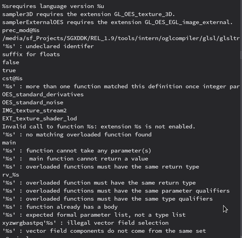
Now, I streamlined my workflow with the tablet quite a bit at this point, I can do a testing cycle quite quickly, but I wanted to see if I could improve it further. So I started taking a look at the PowerVR shader profiling tool, you just need an account to download it. I unpacked it somewhere and noticed a very interesting file "GLSLESCompiler_Series5", other than that there's a fairly well-made GUI to see the assembly for newer architectures and in general profiling shader code generation.
Looking at the symbols in the Series5 binary we can see that they left some function names in for some reason, but it's not really a big deal. If we go to the tab for the strings we see some rather normal-looking compiler errors and OpenGL-related stuff:
But as I scrolled down something caught my eye:
fmad\x00fadm\x00fmsa\x00ffrc\x00frcp\x00frsq\x00flog\x00fexp\x00fsqrt\x00fsin\x00fcos\x00fdp\x00fmin\x00fmax\x00fdsx\x00fdsy\x00fmad16\x00fminmax\x00fmaxmin\x00efo\x00pckf16f32\x00pckf16f16\x00pckf16u16\x00pckf16s16\x00pcku16f32\x00pcku16f16\x00pcku16u16\x00pcku16s16\x00pcks16f32\x00pcks16f16
These look like opcode names, something pretty weird to leave in a binary. My RE tool does not seem to find any references to this data, but it's always good to check with something else, so I tried another one and found the address of a function that does do an indirect reference to it like this:
int32_t sub_8289037(int32_t arg1)
    return *(((arg1 + arg1 + arg1) << 2) + 0x82ceec0)
Seems like that the memory there is a string pointer table stored in a slightly weird way, running the function manually with some different input values yields pointers to the strings in the code block I showed before.
This is already a really large discovery, having opcode-mnemonic mappings can be quite handy, I'd start checking out the opcode names to see if there's anything particularly weird but this function is called from quite a few places, so I wanna check those out first. Along the path I also found some fairly interesting format strings ("%*d: 0x%.8X%.8X\t") and calls to "puts", I used them as a cross-referencing tool to converge to one specific function:
int32_t d?(int32_t* arg1, int32_t arg2, int32_t* arg3)
      int32_t* var_12c = arg3
      void* gsbase
      int32_t eax_2 = *(gsbase + 0x14)
      int32_t var_10c = 0xa
      int32_t var_110 = 1
      while (var_10c u< arg2)
          int32_t edx_3 = var_10c * 5
          var_10c = edx_3 + edx_3
          var_110 = var_110 + 1
      int32_t var_10c_1 = 0
      while (var_10c_1 u< arg2)
          int32_t instr_1 = *var_12c
          int32_t instr_2 = var_12c[1]
          printf(format: "%*d: 0x%.8X%.8X\t", var_110, var_10c_1, instr_2, instr_1)
          char* out
          main_sub(arg1, instr_1, instr_2, &out)
          puts(str: &out)
          var_10c_1 = var_10c_1 + 1
          var_12c = &var_12c[2]
      int32_t eax_19 = eax_2 ^ *(gsbase + 0x14)
      if (eax_19 == 0)
          return eax_19
      __stack_chk_fail()
      noreturn
This look promising. If we look at the call tree of the function we can see that it does indeed call our instruction name function quite a bit, and the first function it calls contains a switch statement based on some field it reads from the instr_n fields (which I labeled myself here).
So, remember that "The Series5 hardware family disassembly compilers are made available upon signing of an NDA."? Whoever was in charge of the "non disclosure" part of enforcing a non disclosure agreement simply removed the function that called the disassembler without actually stripping out the code, and somehow they did not turn on any options in their compiler to garbage collect unused symbols and similar.
So now we have full disassembler code that also seems to do the pretty printing for us, we just have to figure out what the arguments to this function are.
Well arg2 is rather easy, it's just the number of instructions it's going to read, var_12c is just the same as arg3, so that is where the binary is located. arg1 is a little more mysterious. We'll create a structure for it and name if "Info".
After a bit of looking around and labelling things I also found some strings that refer to various PowerVR GPUs followed by binary data, that and the actual disassembler code led me to the following (almost entirely unlabeled) structure:
const uint32_t a[] = {0x13, 0x26, 0x22};
uint32_t a_s = 3;

struct info_unk0 {
	uint32_t				unk1;
	uint32_t				unk2;
	uint32_t				unk3;
	uint32_t				unk4;
	uint32_t				unk5;
	uint32_t				unk6;
	uint32_t				unk7;
	uint32_t				unk8;
	uint32_t				unk9;
	uint32_t const*         unk10;
	uint32_t const*         unk10_len;
	char     const*         name;
};

struct info_unk {
    uint32_t unk;
};

struct gpuinfo {
	uint32_t                type;
	uint32_t                revision;
	struct info_unk         flags;
    uint32_t                padding;
	const struct info_unk0* gpu_info;
};


static const struct info_unk0 data = {
	 0x24000, 0, 1, 0, 3, 1, 4, 12, 3, &a_s, a, "SGX540",
};

#define SGX540 5

static const struct gpuinfo arg = { SGX540, 101, { 0x16b800 }, 0, &data, };
I am not really sure what most of this means, but from what I can see pretty much all of this is specific to each and every PowerVR GPU, and the information for the others is in the binary for future use. What I can say is that very different branches in instruction decoding are taken based on some of this information, even at the "root" of it, which means the architecture changes quite a bit between even GPUs of the same generation/series. Messy.
There are a few ways I could use this, the first one is fully reverse engineering it and rewriting it, but that can come after i understand the architecture more, and since I do know how to call the function I will simply hook into the binary. This actually needs no binary patching, since "__libc_start_main" is a library function that calls the actual main function we can simply hook that with LD_PRELOAD and then call the address the function is loaded at:
((void(*) (void*, uint32_t, uint32_t*))0x082994cb)(&arg, instruction_count, file);
Anyway let's actually disassemble a file, we'll go with the one that added a constant value to the output:
mov.skipinv.repeat3 o0, pa0
mov.skipinv o3, c3
mov.skipinv.repeat2 o4, pa3
emitvtx.end.freep #0 /* incp */, #0
mov.skipinv.repeat3 o0, pa0
mov.skipinv o3, c3
unpckf32u8.skipinv.scale o4, pa3.2, pa3.2, nearest
unpckf32u8.skipinv.scale o5, pa3.1, pa3.1, nearest
unpckf32u8.skipinv.scale o6, pa3.0, pa3.0, nearest
unpckf32u8.skipinv.scale o7, pa3.3, pa3.3, nearest
emitvtx.end.freep #0 /* incp */, #0
fmad r0., r0, r0, r0
mov.skipinv.repeat2 o0, pa0
mov.skipinv o2, c3
mov.skipinv o3, c3
emitvtx.end.freep #0 /* incp */, #0
mov.skipinv o0, pa0
emitst.end.freep #0 /* incp */, #1
mov.skipinv.repeat2 o0, pa0
emitst.end.freep #0 /* incp */, #2
mov.skipinv.repeat3 o0, pa0
emitst.end.freep #0 /* incp */, #3
mov.skipinv.repeat4 o0, pa0
emitst.end.freep #0 /* incp */, #4
mov.skipinv.repeat5 o0, pa0
emitst.end.freep #0 /* incp */, #5
mov.skipinv.repeat6 o0, pa0
emitst.end.freep #0 /* incp */, #6
mov.skipinv.repeat7 o0, pa0
emitst.end.freep #0 /* incp */, #7
mov.skipinv.repeat8 o0, pa0
emitst.end.freep #0 /* incp */, #8
mov.skipinv.repeat9 o0, pa0
emitst.end.freep #0 /* incp */, #9
mov.skipinv.repeat10 o0, pa0
emitst.end.freep #0 /* incp */, #10
mov.skipinv.repeat11 o0, pa0
emitst.end.freep #0 /* incp */, #11
mov.skipinv.repeat12 o0, pa0
emitst.end.freep #0 /* incp */, #12
mov.skipinv.repeat13 o0, pa0
emitst.end.freep #0 /* incp */, #13
mov.skipinv.repeat14 o0, pa0
emitst.end.freep #0 /* incp */, #14
mov.skipinv.repeat15 o0, pa0
emitst.end.freep #0 /* incp */, #15
mov.skipinv.repeat16 o0, pa0
emitst.end.freep #0 /* incp */, #16
mov.skipinv.repeat16 o0, pa0
mov.skipinv o16, pa16
emitst.end.freep #0 /* incp */, #17
fmad r0., r0, r0, r0
mov.skipinv.repeat16 o0, pa0
mov.skipinv.repeat2 o16, pa16
emitst.end.freep #0 /* incp */, #18
fmad r0., r0, r0, r0
mov.skipinv.repeat16 o0, pa0
mov.skipinv.repeat3 o16, pa16
emitst.end.freep #0 /* incp */, #19
fmad r0., r0, r0, r0
mov.skipinv.repeat16 o0, pa0
mov.skipinv.repeat4 o16, pa16
emitst.end.freep #0 /* incp */, #20
fmad r0., r0, r0, r0
mov.skipinv.repeat16 o0, pa0
mov.skipinv.repeat5 o16, pa16
emitst.end.freep #0 /* incp */, #21
fmad r0., r0, r0, r0
mov.skipinv.repeat16 o0, pa0
mov.skipinv.repeat6 o16, pa16
emitst.end.freep #0 /* incp */, #22
fmad r0., r0, r0, r0
mov.skipinv.repeat16 o0, pa0
mov.skipinv.repeat7 o16, pa16
emitst.end.freep #0 /* incp */, #23
fmad r0., r0, r0, r0
mov.skipinv.repeat16 o0, pa0
mov.skipinv.repeat8 o16, pa16
emitst.end.freep #0 /* incp */, #24
fmad r0., r0, r0, r0
mov.skipinv.end pa3, #0x3F800000
fmad r0., r0, r0, r0
fmad.skipinv.repeat4 o0, pa0, c52, c52
emitvtx.end.freep #0 /* incp */, #0
I cut it off at exactly the point where the instructions start being zeros, there's indeed a very large prelude and that there's a further confirmation of instructions being 8 bytes, if we take a look at the subtraction the only difference is this:
fmad.skipinv.repeat4 o0, pa0, c52, c52.neg
Which makes sense, there are is a floating point constant (1.0) but for it isn't actually the one we set in our shader, so that's rather strange. I also suppose that the "emitvtx" instruction does what it sounds like it does (emitting a vertex). Since the register used as an input to the instruction is "c(number)" we can probably assume that there is indeed a set of constant registers, pa0 and o0 are still a bit too nebulous but I suspect "o" might be just output. Now that we're armed with a disassembler we can extract much more useful information out of the architecture, since now we know all the valid instruction encodings and their names but we are not sure what the semantics are. It's much like knowing all the words in a language but not the grammar or the words' meaning.
I will initially just see how common shader constructs are translated to instructions and see what I can infer, based on that it might be a better idea to start looking into making a shader assembly editor (and find or write an assembler) or starting to reverse the actual commands that get sent to the GPU and look into the implementation of actual drawing functions such as glDrawArrays to see how exactly they work.
The next thing I tried is an inverse square root calculation, which resulted in a fairly straightforward translation "frsq.skipinv.repeat4 o0, pa0", the exact internals of the "repeat" flag are still unclear, but a document on the Series6 ISA (which sadly very incomplete) reveals that on it what it does is make an instruction write to 4 consecutive registers, that is the instruction you've just seen writes to o0, o1, o2, o3 this is a fairly unique and interesting way to do SIMD.
The next thing I tried is a sine function in a shader, the output was a bit surprising:
smlsi #1, #1, #0, #0, incrementmode, incrementmode, incrementmode, incrementmode, #0, #0, #0
fmad.skipinv.repeat4 pa0, pa0, sa10, c14
smlsi #1, #1, #1, #1, incrementmode, incrementmode, incrementmode, incrementmode, #0, #0, #0
fsubflr.skipinv.repeat4 pa0, pa0, pa0
smlsi #1, #1, #0, #0, incrementmode, incrementmode, incrementmode, incrementmode, #0, #0, #0
fmad.skipinv.nosched.repeat4 r0, pa0, c38, c34.neg
smlsi #2, #0, #1, #1, incrementmode, incrementmode, incrementmode, incrementmode, #0, #0, #0
efo.skipinv.nosched i2= a0, i0 = m0, i1 = m1, a0=src0+src1 a1=src2+src0, m0=src1*src2, m1=src0*src0, r0, r1, r1
fmad.skipinv.nosched i2, i1, c40.neg, c42
fmad.skipinv pa1, i1, c41.neg, c43
fmad.skipinv.nosched pa0, i1, i2, c44.neg
fmad.skipinv i2, i1, pa1, c16.neg
fmad.skipinv.nosched pa1, i1, pa0, c14
fmad.skipinv pa2, i1, i2, c52
fmad.skipinv.nosched i1, i0, c40.neg, c42
fmad.skipinv pa0, i0, c41.neg, c43
fmad.skipinv.nosched i2, i0, i1, c44.neg
fmad.skipinv i1, i0, pa0, c16.neg
fmad.skipinv.nosched i2, i0, i2, c14
fmad.skipinv i1, i0, i1, c52
fmad.skipinv.nosched i0, i2, r1, c48.neg
fmad.skipinv i0, i0, i1, c48.neg
fmad.skipinv.nosched o1, i0, c52, i0
efo.skipinv i2= a0, i0 = m0, i1 = m1, a0=src0+src1 a1=src2+src0, m0=src1*src2, m1=src0*src0, r2, pa1, r0
fmad.skipinv.nosched i2, i1, c40.neg, c42
fmad.skipinv pa1, i1, c41.neg, c43
fmad.skipinv.nosched pa0, i1, i2, c44.neg
fmad.skipinv i2, i1, pa1, c16.neg
fmad.skipinv.nosched pa0, i1, pa0, c14
fmad.skipinv i2, i1, i2, c52
fmad.skipinv.nosched i1, pa0, r2, c48.neg
fmad.skipinv i1, i1, i2, c48.neg
fmad.skipinv.nosched o2, i1, c52, i1
efo.skipinv i2= a0, i0 = m0, i1 = m1, a0=src0+src1 a1=src2+src0, m0=src1*src2, m1=src0*src0, r3, i0/i0.flt16.0, pa2
fmad.skipinv.nosched o0, i0, c52, i0
fmad.skipinv.repeat2 i0, i1, c40.neg, c42
smlsi #2, #0, #2, #-28, incrementmode, incrementmode, incrementmode, incrementmode, #0, #0, #0
fmad.skipinv.nosched.repeat2 i0, i1, i0, c44.neg
fmad.skipinv.nosched i0, i1, i0, c14
fmad.skipinv i1, i1, i2, c52
fmad.skipinv i0, i0, r3, c48.neg
fmad.skipinv i0, i0, i1, c48.neg
fmad.skipinv o3, i0, c52, i0
emitvtx.end.freep #0 /* incp */, #0
Well this confirms that this actually does not have an instruction for sine, this code is in one way or another computing a sine. We don't have enough information to know exactly what is going on here but we can see that instructions can take quite a few more operands than what you'd see in a traditional architecture. Also of note is that so far every shader has started with the same 82 instructions and ended with the same instruction (with a ".end" suffix).
OpenGL shaders have a way to pass custom data between vertex shaders and fragment shaders called "varying", as the name suggests this value can be different for each vertex, and by default for pixels that are in-between vertices it gets interpolated. This is a fairly powerful tool since vertex shaders don't really have many builtin-in outputs. With this I tested a shader that is a bit more complex than the ones I've shown so far, they make use of both varyings for the output of vertex shaders and uniforms for the inputs (uniforms are values that are constant but may vary between different calls to a draw function):
gl_Position = vPosition + vec4(0.2, 0.873, 0.592, 0.987) + a + b + s + v;
o = (vPosition + vec4(0.2, 0.873, 0.592, 0.987) + a + b + s + v).x;
Here's the disassembly for this one
fmad.skipinv.repeat4 pa0, pa0, c52, sa20
smlsi #1, #1, #0, #0, incrementmode, incrementmode, incrementmode, incrementmode, #0, #0, #0
fmad.skipinv.repeat4 pa0, pa0, c52, sa10
fmad.skipinv.repeat4 pa0, pa0, c52, sa11
smlsi #-1, #1, #0, #1, incrementmode, incrementmode, incrementmode, incrementmode, #0, #0, #0
fmad.skipinv.nosched pa0, pa0, c52, sa12
fmad.skipinv.repeat3 i2, pa1, c52, sa14
smlsi #1, #-1, #0, #1, incrementmode, incrementmode, incrementmode, incrementmode, #0, #0, #0
fmad.skipinv o0, pa0, c52, sa13         ; compute first component of the output
fmad.skipinv.repeat3 o1, i2, c52, sa17  ; compute the remaining components
mov.skipinv o4, o0                      ; set "o"
emitvtx.end.freep #0 /* incp */, #0
That smlsi instruction definitely looks interesting, not quite sure what's going on with that one. Based on the repeat counts it's not hard to figure out which fmad is doing what (of interest is sa, there's also pa, could these be primary and secondary?), we also see another new kind of register "i", not sure what that could be for now.
Let's do a slight variation now:
gl_Position = vPosition + vec4(0.2, 0.873, 0.592, 0.987) + a + b + s + v;
o = (vPosition + vec4(0.2, 0.873, 0.592, 0.987) + a + b + s + v).y;
Assembly:
fmad.skipinv.repeat4 pa0, pa0, c52, sa20
smlsi #1, #1, #0, #0, incrementmode, incrementmode, incrementmode, incrementmode, #0, #0, #0
fmad.skipinv.repeat4 pa0, pa0, c52, sa10
fmad.skipinv.repeat4 pa0, pa0, c52, sa11
smlsi #-1, #1, #0, #3, incrementmode, incrementmode, incrementmode, incrementmode, #0, #0, #0
fmad.skipinv.nosched pa0, pa0, c52, sa14
fmad.skipinv.nosched.repeat2 i2, pa1, c52, sa12
smlsi #1, #-1, #0, #5, incrementmode, incrementmode, incrementmode, incrementmode, #0, #0, #0
fmad.skipinv i0, pa3, c52, sa16
fmad.skipinv o0, pa0, c52, sa17
fmad.skipinv.repeat2 o1, i2, c52, sa13
fmad.skipinv o3, i0, c52, sa19
mov.skipinv o4, o1
emitvtx.end.freep #0 /* incp */, #0
I expected this to actually be just the previous block of code with o1 used in instruction 92 rather than o0, there has to be some extra limitation we're not aware of.
We can see two main differences, at instruction 88 instead of repeating 3 times it repeats the add 2 times, and the last add is done in 3 steps instead. If we instead do this with the z component the only change is on instruction 94, changing the register to o2, my assumption is that there is a delay between a repeat instruction being executed and the output from it being available.
One way to determine exactly the nature of this output is getting the compiler to generate a wider fmad operation and using different outputs from it. I can think of a few ways to accomplish this, but at this point I have a fairly decent understanding of how the "processing" parts of vertex shaders are implemented, from a cursory look at fragment shaders they seem to have less instructions at the start but they are largely similar.
At this point I want to start looking into exactly how rendering works on this outside of shaders, how and where shaders are loaded on the device, how is geometry data sent to the device, things like that.
Reverse engineering other driver code
Here I decided to try something new, I switched to using frida to write my tooling in order to accelerate development a bit, I actually learned about it from a friend as I was about to start working on this other phase of the project.
First of all I wanted to see how exactly glUseProgram was implemented, this function sets the current set of shaders used for drawing to the screen
void glUseProgram(int32_t newProgram)
  int32_t lr
  int32_t var_4 = lr
  struct OpenglContext* ctx = getOpenglContext()
  if (ctx == 0)
      return
  void* program = ctx->currentProgram
  if (program != 0 && *program == newProgram)
      return
  if (newProgram == 0 && program == 0)
      return
  return setCurrentProgram(ctx: ctx, program: newProgram) __tailcall
After some analysis this is what I ended up with, the setCurrentProgram subroutine simply runs some basic checks and sets the current program and a flag that is later checked (and unset) during glDrawArrays. From this information we can gather that this flag is likely a "dirty" flag that signals that shaders have been changed and must be uploaded to the GPU again.
We can verify this hypothesis by using MemoryAccessMonitor from frida to warn us of writes to areas that have been mapped to shader code, or rather we would be able to do that if it were supported on Android. So let's implement our own solution, we can simply use "Memory.protect(addr, size, 'r--')" to make all writes to the memory area throw an exception, so we write some simple code that just alerts us of writes for now, we run it and... the tablet instantly reboots. I did a few more attempts and the issues seems to be that some shader memory areas will simply bring the entire system down is mprotect-ed when an exception happens, which is a fairly severe issue, one shouldn't be able to bring an entire system down with a simple 3D application.
So what are our options now? We can either hook a call that is likely used to write to the memory, or use single-stepping. Frida actually offers an API called "Stalker" that allows for very fine-grained inspection and modification of the instruction stream, but for now I picked to simply hook all memory copies and checking whether their destination is within one of the areas of memory mapped to GPU code.
After tying all of the code together to do this I found something very interesting, there were many memory copies to fragment shader code, but vertex shader code only had 2 (one for each time we change the shader) and both were at offset 0x290, if we divide this offset by the instruction size we get 82, exactly the number of "prelude" instructions that we found before! Curiously there are no memcpys to previous area of code, so one might thing that the code there is just some garbage that somehow ends up being consistent, but removing it ends with hanging the GPU and once again bringing down the entire system.
Now I could go and make the other tracing approach to catch the remaining writes with frida, but I wanted to see about moving to PostmarketOS since I was starting to get a bit annoyed with Android.
Getting the alternative OS on the device just required me changing some packages around due to PowerVR GPU acceleration support being dropped officially due to proprietary drivers being quite hard to maintain, after a bit I managed to get it running, the only minor annoyance is the fact that the charger is not supported, so if I am doing something particularly heavy the device will end up discharging faster than it charges. The second issue is that frida only provides binaries that work on glibc, now one would think that the solution would be as simple as either compiling it on the device for musl or using a cross-compiler. The issue is, frida has a very interesting idea of how it should be built, it sets up the entirety of its own toolchain (which does not include a compiler for some reason), has outdated documentation on how to port it to other systems (while clearly this has been done before, it can run with uclibc on mips) and is in general a major pain to try and compile. After 2 days of trying to get it to build for musl I gave up and rewrote my tooling instead.
Now that that's handled I'd like to track the remaining writes, so we need to use some sort of "watchpoint" functionality. Ideally one should be able to raise a SIGSTOP followed by a SIGTRAP and attach gdb, but that makes gdb crash and makes the graphics driver crash, so once again the easy solution does not work, so let's get to work. We'll use "mprotect" to make sure that every access to the memory areas of interest raise a signal (the same one that normally causes a segmentation fault).
After we catch the signal we want to log the memory access, but it's also important that we actually do run the instruction that accessed it. As things stand now if we return we'd simply end up getting back in the handler immediately. We could parse the instruction and manually perform the access but that'd be rather complicated. Instead we can make it so upon return the access will not cause a signal, but the next instruction will cause a SIGTRAP, which will be caught by another handler, which will make it so the memory will cause a signal again and also re-write the instruction to be the one that was in the spot before.
Two issues I encountered with this part were that the code was actually THUMB rather than ARM and that ARM's instruction cache needs manual clearing, other than that it went rather smoothly.
saved_instruction = 0;
fault_addr = 0;

void sigsev_handler(info) {
    //get exact offset in library and print it out
    //make the memory writable
    mprotect(PAGE_ALIGN(infoaddress), PROT_READ | PROT_WRITE);
    addr = PAGE_ALIGN(return_address);
    //make the code writable so we can make the next instruction
    //go back into our code after the memory access is done
    mprotect(addr, PROT_READ | PROT_WRITE | PROT_EXEC);
    fault_addr = addr;
    //thumb2 has variable instruction length
    addr += get_instruction_size(addr)
    //this will cause a sigtrap
    //which will call the handler after this one
    saved_instruction = *addr
    *addr = breakpoint
}

void sigtrap_handler() {
    //make the next access fault
    mprotect(addr, PROT_READ);
    //restore previous instruction
    *return_address = saved_instruction;
    //dump the intermediate shader
}
Now we have about 140 intermediate shader dumps and a log of every single offset that performed a write to the vertex shader area, each of them with 4 bytes of difference from the previous one. After this we can easily check that we did indeed get every single write to the memory area we are monitoring, it's also interesting that after a bit of processing we can see that all the writes are eventually handled by 4 unique functions.
If we want to be more accurate we're going to have to build some form of correspondence between OpenGL calls and memory writes, which for now I have done by simply inserting some printfs in my testing program. This reveals that most of the writes are made far before any of our logging even runs, except for the last 24 bytes (3 instructions) of shaders. The solution I wrote for now only tracks one memory area which is quite restrictive, but now we have a far more precise view of where code for vertex shaders is generated.
302:override PDSASM := $(if $(V),,@)$(HOST_OUT)/pdsasm
Another assembler? There's overrides for other programs, including useasm, which is obviously the USE assembler, there's likely another ISA on the GPU, much like ARM with Thumb (at least version 1 of it). There's a few relevant strings in the main driver binary, "WritePDSVertexShaderProgramWithVAO", same goes for pixel shaders. There are a few other software distributions by the manufacturer that seem to reveal some very basic PDS opcodes, specifically shifts, movs and some sort of "special mov" (probably).
After this I also followed the call chain for glDrawArrays (which is strangely much simpler on postmarketOS), and found that the way this is all started off is a call to SGXKickTA, which eventually calls the kernel code. Here we find something interesting, there's references to "kicking the ukernel", according to the documentation provided by the manufacturer the GPU microkernel only handled some low level power management tasks, but that might not be quite accurate.
If we take a look at the init scripts for postmarketOS we can find something interesting, there's a binary called "pvrsrvinit", the binary is fairly trivial and just links to "libsrvinit.so", which allocates some memory in the "kernel" area of GPU memory and writes a few static binaries to it, and luckily they're also associated with a name "3D, SPM, TA, ukernel". This seems to tell a very different story from what the manufacturer said, I am not sure about SPM, but 3D is fairly obvious, TA refers to the tile accelerator, a component in powerVR GPUs, and ukernel is likely the main kernel binary.
We can disassemble the binaries and find some interesting things, first of all there are multiple instruction sequences that are of this general structure:
mov r2, #0xDEADBEEF
mov r4, #0x00000000
emitpds.tasks.taske #0 /* incp */, r0, r2, r4, #0x00000843
And looking at the remaining initialization code, the "DEADBEEFs" are later patched with values based on other addresses, so it is likely that it's the address of actual PDS code, which will be useful later.
Also at this point I generalized the backend for memory tracking to support multiple memory areas, it actually wouldn't be hard at this point to expand it to be an armv7 debugger library.
Now i need to track running code on the GPU and extract the values of registers or pause execution (essentially a debugger), the easiest way to do this is via shared memory, since at this point I have an disassembler but not an assembler I will have to go based on the disassembly I have access too and a bit of perturbation to figure out the necessary opcodes. One first look at the kernel binaries reveals specifically that integer operations seem to all be collapsed in a single instruction called "imae" with quite a few arguments, while floating point operations look a lot more approachable.
The plan is to write code that works roughly like this:
store register to known memory address
notify the CPU
wait for the CPU to confirm that it has read the register
So we need to know how to do stores, loads, conditionals and branches. Here is where I found out something, the disassembler simply doesn't show some of information that is necessary to actually encode a valid instruction, and additionally invalid instructions will simply be skipped during execution. After quite a bit of bit shuffling I was able to encode the following:
mov r3, #0x0
stad.bpcache [r3,+#2], #1
Which moves a 32-bit immediate (which has its own quite weird encoding) into a register, and then stores "1" as a doubleword (32 bits) to the memory located at "r3 + 2 * 4", the meaning of the bpcache is likely "bypass cache". After hijacking an allocation to get a memory area that no other code will touch I ran this code with a correct immediate and I finally was able to see some results from this GPU, now we need loads, conditionals, branches and float operations.
Note that i replaced the immediate with a valid memory address i allocated by hijacking one of the memory allocations.
After quite a bit of trial and error and educated guesses I figured out the encodings for all of these, and came up with the following instruction sequence:
mov r3, #0x0D803004
mov r5, (x)
stad.bpcache [r3,+#0], r5
stad.bpcache [r3,+#2], #1
ldad.bpcache r4, [r3,+#1], drc0
wdf drc0
mov r5, c52
fsub.testtaz.chan0 r1, p2, r4, r5
!p0 br -#0x00000004
Before I can explain what this does a few details are needed, loads have an extra "drc" argument, which seems to be some form of "barrier" that one can wait on with wdf to check that the load has gone through. Now we get to how branches actually work, each instruction can be prefixed with a predicate register (which may be negated), which stores a boolean that indicates whether the instruction should run or not, some instructions are able to be suffixed with "test flags" that write to said predicate registers based on some conditions (in this case, if a floating-point subtraction has a zero result), we can use this predicate to prefix a branch instruction and loop until the CPU confirms that it has read the register. Of course the CPU part of this has to run in a separate thread, because for now I am testing this with a shader, and this will make glDrawArrays pause until the loop is over.
Surprisingly this ended up working on the first attempt after I tested each instruction singularly, now we have a way to dump arbitrary registers as long as we have space to put this code.
Thankfully all memory areas seem to have quite a bit of extra space leftover, still due to the sheer number of registers that are encodable (which don't necessarily have to correspond to actual registers given that GPUs tend to have variable amounts of registers per thread), the code would be quite large (8 bytes per instruction, 8 instruction that are necessary, 7 register banks, each of them has 128 registers, which makes 57344 bytes to dump them all), so moving forward I'll probably rework the protocol slightly to allow for modifying the second instruction in the loop. Something else that needs to be considered is that we cannot actually dump all the registers since some of them are necessary to dump others in the first place.
Another important piece of information i want is finding the entry points of the kernel code, which can be done by replacing relevant portions with memory stores that endlessly loop and reading the memory from the cpu.
This for now summarizes the current state (as of commit a0ece45ba7) of the project, the next step would be finding the best way to track kernel code and in general insert calls to the register dump code at any arbitrary spot, which actually only requires wasting one register for the address and storing all the others to memory. There's still quite a lot of work to be done, the mechanism to actually render graphics and start threads is entirely unknown, and while I could simply use the already existing microkernel and replace the userspace graphics library I don't feel that would make sense in the context of making a fully open source driver, so i am going to also try to develop a replacement microkernel after reverse engineering it.
The code can be found here